Experimental design
The objective of this study was to increase the long-term stability of thin-film-based intraneural electrodes eliciting sensation in human arm nerves and to the analyze their performance and integrity after up to six month of application.
Design considerations of the thin-film electrodes
The design of the thin-film TIME passed through various changes in its applications since the very first idea in 2008 (Fig. 7). From the early in vitro and acute in vivo experiments in rats with the TIME-1, we rapidly learned some basic pre-requisites of implantation and fixation which were implemented within the further small and large animal implants TIME-2 and TIME-3, respectively.
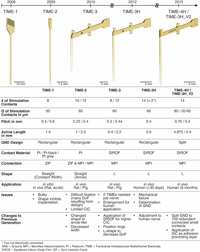
TIME-2 was mostly used in small animal experiments, proving biocompatibility of the used materials29 and showing advantages in the stimulation selectivity19. TIME-3 implants were used mainly in large nerves of pigs30,31. SIROF was applied as contact material to increase the charge injection capacity and thus increase the stimulation safety limits14,45. In a first-in-human study the TIME-3H showed excellent clinical outcomes1,32, but as well weak points concerning the mechanical integrity, especially of the ground contact sites33. SiC was introduced as adhesion promoting layer and the large area ground contact site was split into 109 redundant connected small contact sites.
The implant version TIME-3H proved feasibility as an adequate peripheral nerve interface used for sensory feedback during the first sub-chronic human clinical trial1,32. The clinical outcome and the electrical stability of the implants were excellent. Due to explantation and subsequent handling of the thin-film electrodes, weak points were identified, especially concerning the mechanical integrity of the rectangular ground contact sites. As a first consequence, silicon carbide was introduced as an adhesion-promoting layer between the PI and platinum. This updated layer setup was tested and verified in vitro40 and in vivo (small animal model) with regard to chronic application33.
In order to improve the thin-film electrodes towards chronic implantation up to six months in humans, we made also some design considerations to lower intrinsic stress in the thin-film metallization, and thereby the risk of delamination, thus increasing the safety for the patient.
The TIME-3H14,33 was consistently further developed up to the design freeze for the chronic human implantations, keeping fundamental design elements and changing details to improve the mechanical stability. The fundamental design elements were the two-dimensional U-shape for fabrication, which is transformed into a L-shape after folding during assembly. Details are described elsewhere14,33. Further fundamental design elements were realized with the thin-film sectioning. It consisted of three parts: the electrode, ribbon and transition part (Fig. 8a). The electrode part contained the active strip with 14 stimulation sites incorporated (seven per side) and after folding a loop with an integrated surgical needle and thread. Positioning, pitch and size of the stimulation contact sites were depending on the thin-film version. The stimulation contact sites were labeled from the ribbon part towards the middle line L1 to L7 and R1 to R7 (Fig. 8a). The ribbon part contained all tracks, which led from the transition part to the stimulation contact sites and the large area ground sites, named L GND and R GND. The transition part had incorporated a structure to interconnect the thin-film electrode with a subsequent helically wound cable. The Microflex interconnection technique (MFI)41 was used as a robust and reliable technique to assemble a thin-film ribbon with a long helically wound cable (Fig. 8a). The focus of the current designs was placed on the large electrode area of the ground contact sites (see simulation sections). The ground contact sites are of fundamental importance, as a failure would lead to a total malfunction of the implant. The aim of the redesign was to prevent stress due to the large continuous area and rectangular edges, but to keep an area as large as possible to ensure an electrical closed-loop for stimulation. To preserve these boundary conditions, the rectangular ground site was split to 109 interconnected circular contacts with an exposed diameter of d = 80 µm (Fig. 8a, red box) (diameter under polyimide d = 100 µm) of a single site. The contacts were arranged in a hexagonal assembly with a pitch of 125 µm in three rows. Eliminating large continuous areas and replacing highly stressed rectangular edges by round shapes should decrease the intrinsic stress of the thin-film metallization and thus decreasing the risk of delamination. A further advantage of the design, in case of partial damage, was the structural resilience of the design. The remaining ground contact sites would be still functional as every contact of the ground is electrically connected among each other. Concerning the active strip, two designs were developed, resulting in the TIME-3H_V2 and the TIME-4H. Both were manufactured with the split ground contact sites.
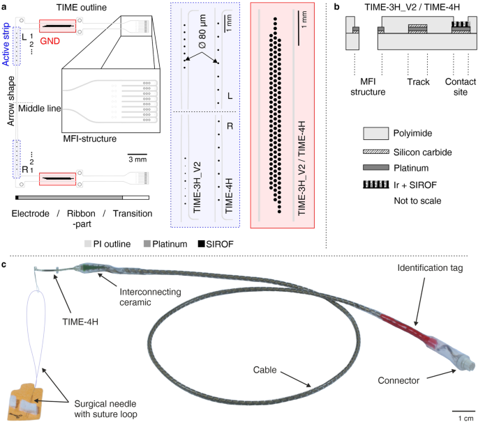
a Two different designs for the active strips were realized (blue box). The ground contact site was split to 109 circular redundant connected contacts with a single diameter of 80 µm (red box). b The layer setup of both designs was chosen identical. c In the assembled TIME implant a surgical needle with a suture was incorporated within the thin-film loop (TIME-4H). The polyimide-based thin-film electrode was attached via the MFI technique to an interconnecting by use of screen-printing structured ceramic. To this in turn 16 helically wound MP35N- wires covered by a medical-grade silicone rubber hose were soldered and terminated on the opposite side in a commercial connector. Colored silicone rubber and an identification tag made of laser-structured platinum were used for distinct identification.
The TIME-3H_V2 was conceptualized in a way, that the left side of the electrode had integrated seven standard active sites with a diameter of 80 µm. However, the right side exhibited from the ribbon part downwards on the active strip decreasing the diameters of the active sites. The diameter started at 60 µm and decreased with 20 µm steps down to a diameter of 20 µm and starting again at 60 µm. In the folded state, the active sites were directly opposite to the left side. The active strip had a length of 2.4 mm, resulting in a contact site pitch of 0.4 mm.
The design of the active strip within the TIME-4H was developed in way to cope a larger area / diameter of the targeted nerve with a single electrode, as for this type of implant the surgical protocol was slightly different42. Considering that using directly opposite stimulation sites would mean one fascicle is addressed by two active sites, a shift of half the pitch (in this case 0.75 mm) of left and right side of the electrode was included to potentially address more fascicles with the same number of active sites. Otherwise the standard size for the active sites of 80 µm in diameter was used.
In both versions, platinum tracks and pads were sandwiched between polyimide as substrate and insulation layer (Fig. 8b). Silicon carbide (SiC) was used as an adhesion promoter between platinum and the PI substrate. Platinum tracks were completely surrounded by the SiC and polyimide (details below). At the active sites and ground contacts, the platinum layer was coated by iridium, subsequently covered by a sputtered iridium oxide film (SIROF) and opened via reactive ion etching (RIE). The MFI structure exhibited SiC only between platinum and the lower PI layer, in order to have bare platinum on the MFI ring after RIE opening for mechanical adhesion within the assembly procedure.
The detailed implantation procedure is described elsewhere1,14. In general, the front part of the TIME design (active part) is pulled with the incorporated needle and suture during the implantation through the nerve. The active sites for stimulation have to lay inside the nerve. The fixation flaps and the loop are sutured to the surrounding tissue, for the purpose of avoiding movements of the electrode during daily life.
Simulation of intrinsic mechanical stress
Thermo-mechanical intrinsic stress was simulated using COMSOL Multiphysics® (version 5.3, COMSOL Inc., Burlington, MA, USA). If not otherwise stated, standard parameters given by the software were applied.
Two concepts of the large area ground contacts were designed. First, a rectangular design used for the TIME-3H14,33, i. e. with an exposed metallization area of 1 mm × 0.25 mm (A = 0.25 mm2) and second, a split ground with 109 circular exposed metallization contacts with a diameter of d = 0.08 mm (A = 0.55 mm2). For simplification, a polyimide-platinum sandwich was simulated without adhesion layers and without SIROF. Platinum is the main conductive material, representing the tracks, MFI structures and the base of the stimulation and contact sites. If failure occurs within the platinum structure, the whole device is prone to failure.
Minimizing the intrinsic stress in the platinum layer is of the highest relevance. SIROF however serves only as enhancement of the charge transfer to the tissue.
The geometries were designed in SolidWorks (Version 2014, Dassault Systemes Deutschland GmbH, Stuttgart, Germany) and imported in COMSOL Multiphysics®. Parameters of both materials, polyimide and platinum were acquired via the internal “MEMS” materials library (changed parameters are listed in Fig. 2c). Several boundaries from the “Solid Mechanics” and “Heat Transfer in Solids” from the internal definitions were applied. An external temperature of 394.15 K as heat flux boundary was chosen according to the sterilization process performed after assembly (not 723.15 K imidizing temperature, since the metallization is homogeneously sandwiched between closed PI layers within this process step). A free tetrahedral mesh was used with custom-changed mesh sizes.
Cleanroom fabrication of thin-film electrodes
The microfabrication of the TIME thin-film electrodes was conducted in a cleanroom environment using standard photolithographic and MEMS processes (Supplementary Fig. 1). Details are described in the supplementary material and elsewhere14,33. All thin-film electrode designs described above feature polyimide (PI; type: biphenyldianhydride / 1,4-phenylenediamine BPDA-PPD) as substrate and insulation material. MEMS processes utilized were plasma-enhanced chemical vapor deposition of SiC (PECVD, PC310 reactor by SPS Process Technology Systems Inc, San Jose, CA, USA), evaporation of Pt (Leybold Univex 500, Leybold Vacuum GmbH, Cologne, Germany) and sputter deposition of Ir and IrOx (Leybold Univex 500, Leybold Vacuum GmbH, Cologne, Germany). After the last fabrication step, the thin-film electrodes were pulled off the silicon wafer with a pair of forceps (Supplementary Fig. 1g) for assembly of the implants.
Chronic human implant
The TIME-3H_V2 and TIME-4H implants (called TIME implants if specification not relevant) were assembled out of four sub-modules (Fig. 8c; for details see14). First, the thin-film part containing the contact sites for stimulation and the ground contacts to close the electrical circuit. Second, a screen-printed interconnecting ceramic to mechanically and electrically connect the thin-film electrode to the third part, a 40 cm long cable. The fourth module was a commercially available connector (NCP-16-DD, Omnetics Connector Corporation, Minneapolis, USA).
The fabrication procedure was similar to the fabrication procedure of the TIME-3H (details in14,33) with little adjustments due to chronic application in human (details in supplementary materials).
After some connector issues, with regard to strain relief during daily handling, loosing channels within the first two patients7 the connector assembly was strengthened using a protective rubber hose (NuSil MED-4750, Freudenberg Medical Europe GmbH, Kaiserslautern, Germany) at the wire-connector transition (Fig. 8c) for patient 3.
The TIME implants were fabricated within the fully ISO 13485-certified Laboratory for Biomedical Microtechnology of the Albert-Ludwig-University of Freiburg, Freiburg, Germany. Before implantation, each TIME was hydrated in order to increase the charge injection capacity43, characterized and tested on functionality. Afterwards, it was washed, wrapped in sterile bags, labelled and steam-sterilized at 121 °C and 2 bars for 21 minutes. The stimulation and ground contact sites of all delivered implants were fully functional.
Within clinical trials, MRI investigations are of interest and therefore the state of MRI compatibility of implants is relevant44. Medical devices can be declared according to the ASTM standard F2503 MR safe, MR conditional and MR unsafe. We have used the F2503-08 version while the F2503-13 was released after our examinations had been finished. Investigation according to the relevant standards (ASTM F2052-14, F2213-06 & F2182-11a) have demonstrated that the TIME-4H implants (in clinically relevant position and orientation according to manufacturer specification) can be considered “MR conditional”. Meaning, a patient with these devices can be safely scanned in a MR system meeting the following conditions; 1) static magnetic field of 3 T, with 2) maximum spatial field gradient of 25700 Gcm−1 (257 Tm−1) and 3) maximum force product of 441 T2m−1.
Under the scan conditions defined above, the TIME-4H electrode is expected to produce a maximum temperature rise of <0.5 °C (2.3 Wkg−1, 3 T) RF-related (switched gradient during imaging) temperature increase with a background temperature increase of <0.1 °C (2.3 Wkg−1, 3 T).
Human clinical trials
Human clinical trials were performed in three patients according to European Law between 2015 and 2017. This study was conducted as part of the clinical trial NCT02848846 (https://clinicaltrials.gov/). Electrodes were explanted at the end of the trial periods. Details are described in the supplementary material.
Electrochemical electrode characterization
In order to compare the electrochemical properties of the TIMEs before implantation and after explantation the devices underwent a characterization with electrochemical impedance spectroscopy (EIS) in vitro. The characterization was carried out with a frequency analyzer and a potentiostat (SI 1260 & SI 1287, Solartron Analytical, Farnborough, UK) in phosphate-buffered saline (PBS) solution with a voltage amplitude of 10 mV and a frequency range of 100 kHz to 1 Hz. The three-electrode setup consisted of an Ag/AgCl reference, a large area platinum counter and the respective stimulation or ground contact sites of the TIME implant as working electrode. Beforehand, the SIROF was hydrated via cyclic voltammetry43, using the identical setup as used within EIS. The voltage sweep was performed between −0.6 V and 0.8 V, with 200 mV steps for 250 cycles.
Three neural stimulators: STIMEP (INRIA, Montpellier, France & Axonic, Vallauris, France), EARNEST (University of Cagliari, Italy) and the Grapevine Neural Interface System (Neural Interface Processor, 512 Channels of Potential, Ripple LLC, Salt Lake City, UT, USA) were used to inject current into the nerves of the subjects by means of TIME implants (details are provided in the supplementary materials). For the characterization of the electrode-nerve impedance in vivo and the subjects’ response to intraneural stimulation, we delivered trains of cathodic-first, biphasic and symmetric square-shaped, current-controlled stimulation pulses of variable intensity, duration, and frequency, through a dedicated software controlling one of the before mentioned, external, electrical neural stimulators. The impedance in vivo was estimated as the ratio between the potential difference between the selected stimulation contact site and the ground contact sites (both, left and right one of the electrode) at the end of the cathodic pulse phase divided by the current pulse magnitude. The potential resulted from the average of four pulses (the first one of a five-pulse train was removed) with a current amplitude of 20 µA and a pulse width of 300 µs, repeated at a frequency of 1 Hz. While a safety margin has been applied in functional assessment in the patients7, this paper uses 150kΩ as maximum impedance for the definition of electrically functional stimulation contact sites which corresponds to the maximum output swing of the stimulators.
Optical analysis of explanted thin-film electrodes
The optical analysis of the stimulation and ground contact sites were done using light microscopy with polarization filters (Leica DM400M, Leica Microsystems GmbH, Wetzlar, Germany) to enhance visualization of surface irregularities and changes in adhesion (Fig. 4b, left column).
White light interferometry (WLI; Wyko NT9100, Veeco Instruments Inc., Plainview, NY, USA) was used to quantitatively investigate the topography in three dimensions (Fig. 4b, middle columns).
In accordance to analyze the properties of the layer setup, scanning electron microscopy (SEM) in combination with focused ion beam (FIB; Zeiss Auriga 60, Carl Zeiss AG, Oberkochen, Germany) was utilized to gather high-resolution overviews of the contact sites and to cut cross-sections into the thin-film metallization.
Five categories of stimulation contact site status were defined in order to obtain an objective classification (Fig. 4b). Category 1 represents a contact which can be compared to a pristine one, meaning from a material (not electrical) point of view, fully functional, with perfect adhesion and perfect surface integrity. Category 2 exhibits signs of delamination of ≤1 µm (distance between metal and underlying polyimide substrate) and / or (possible) light crack formation in the contact site coating. Delamination between 1 µm and 6 µm and crack formation occurs in category 3. Partial delamination of a metallization layer is categorized as cat. 4. The highest impact of destruction occurs in category 5 with heavy delamination of >6 µm, disintegration of the metallization layers or compression or destruction of the PI substrate.
For comparison reasons, 15 stimulation contact sites identical to TIME stimulation contacts were stimulated using a pulse generator up to 6.5 billion times. The test was performed using a two-electrode setup. A large area platinum counter electrode and the TIME-like stimulation contacts were used as working electrodes in PBS solution, as well as a stimulator (PlexStim Electrical Stimulator, Plexon Inc. Dallas, TX, USA) and a pH-meter (pH-Meter, Qph70, VWR International GmbH, Darmstadt, Germany) to monitor the pH-value during the stimulations. A rectangular charge-balanced pulse form was applied, cathodic first with a pulse width of 200 μs, 10 μs pulse delay and a repetition frequency of 500 Hz. The amplitude was set to 578 μA which was calculated based on the safe charge injection limit of SIROF (2.3 mCcm−2) to avoid overstimulation14. Gathering the voltage response using a picoscope (PicoScope 2000 Series, Pico Technology, St. Neots, UK) and evaluation of its data using MATLAB (MATLAB, The MathWorks, Inc., Natick, US).
To gather compound overviews of the ground contact sites with a high degree of details, images with a tabletop SEM (Phenom Pro Desktop SEM, Thermo Fisher Scientific Phenom-World B.V., Eindhoven, Netherland) were acquired and highlighted with CorelDRAW X7 (Corel Graphics Suite X7, Corel GmbH, München, Germany).
Connector analysis
Issues with the connector assembly occurred as already mentioned above. During daily handling (connection and disconnection of the extracorporeal stimulator) many channels were lost. After scheduled termination of the clinical trial, the implants were retrieved. The connectors were analyzed with regard to the electrical state and the mechanical integrity. The electrical state was tested with a resistance meter (34401 A 6 ½ Digit Multimeter, Agilent, Santa Clara, CA, USA) between different tapping points (connector – solder pads on interconnecting ceramic – wires anterior to interconnecting ceramic). Mechanical integrity at the wire-connector transition was investigated using µ-computer tomography (µ-CT; Nanotom m, GE Sensing & Inspection Technologies, Wunstorf, Deutschland) (Fig. 5). Using this technique, x-ray images were acquired in all three dimensions throughout the wire-connector transition (Fig. 5b). In case of a ruptured wire from the connector there is no white dot representing the cross-section of a wire visible at the transition position (Fig. 5b, upper grey image). In the lower transition image in Fig. 5b all 16 wires a visible.
Statistical analysis
Statistical methods were applied for data analysis of the electrochemical experiments. The data acquired in vivo was longitudinal and unbalanced for each time point (weeks). Moreover, the data was not normal distributed and the variance was not homogeneous as well. Therefore, we applied a linear mixed effect model using the software R (version 3.5.2, The R Foundation for Statistical Computing, Vienna, Austria) and RStudio (Version 1.1.463, RStudio Inc., Boston, MA, USA), which is robust to non-normality and unbalanced data sets. Further detailed statistical analysis of the impedance data was performed elsewhere7.
A non-parametric Kruskal-Wallis method was applied, to assess differences between the impedances classification, comparing optical and electrochemical data.
- SEO Powered Content & PR Distribution. Get Amplified Today.
- PlatoData.Network Vertical Generative Ai. Empower Yourself. Access Here.
- PlatoAiStream. Web3 Intelligence. Knowledge Amplified. Access Here.
- PlatoESG. Carbon, CleanTech, Energy, Environment, Solar, Waste Management. Access Here.
- PlatoHealth. Biotech and Clinical Trials Intelligence. Access Here.
- Source: https://www.nature.com/articles/s41528-023-00284-x